


How to Reduce Parasitic Capacitance in a PCB Layout

At a Glance
Learn how to reduce parasitic capacitance so you can prevent high-frequency noise coupling in your PCB layout.


Noise in an electronic system comes in many forms. Whether it’s received from an external source or it transfers between different regions in a PCB layout, noise can be unintentionally received via two methods: parasitic capacitance and parasitic inductance. Parasitic inductance is pretty simple to understand and diagnose, both from the perspective of crosstalk and from coupling of apparently random noise between different sections of a board.
Parasitic capacitance is not necessarily more difficult to deal with, but it does require understanding how PCB layout geometry will affect mutual capacitance. In systems operating at high frequencies or where high dV/dt nodes can create capacitive noise coupling, some simple PCB layout choices can help you reduce parasitics. In this article, I’ll describe generally how to reduce parasitic capacitance and provide some examples in high-frequency routing, as well as in a switching converter.
Identify and Reduce Parasitic Capacitance
While there is no single formula for parasitic capacitance, it has a general definition:
- Parasitic capacitance is the unintentional capacitance (and generally unwanted) that exists between two conductive structures that are separated by an insulator.
Sometimes, this unintended capacitance is actually beneficial, and in such cases we don’t use the term “parasitic” to describe it. Take a power-ground plane pair for example; this simple structure helps provide a large charge reservoir to support high speed components with high I/O count because of its inherent capacitance. Another example would be in a coplanar waveguide, where you basically take advantage of the parasitic capacitance to set the impedance of the interconnect to a required value.
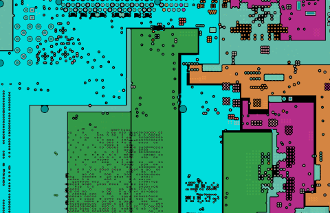
In a PCB, parasitic capacitance can appear essentially anywhere. Take a look at the layout below; I’ve called out some areas where parasitic capacitance is prominent. This only shows the capacitance generated on the top layer, but there could be capacitance on any layer.

Just as the definition above suggests, parasitic capacitance arises between any pair of conductors separated by a dielectric, and we can quickly identify multiple areas where parasitic capacitance appears in the above example. Whenever you have parasitic capacitance in a PCB layout, it can arise in two ways:
- As self capacitance, which appears as a high undesired capacitance between a conductor and a different conductor (usually GND).
- As mutual capacitance between two conductive structures that are each referenced to a 3rd conductive structure; this is effectively the form of capacitance that causes capacitive coupling between two traces.
Why does high parasitic capacitance matter? It matters because, whenever there is a changing potential between two capacitively coupled conductors, this causes some displacement current to flow on each conductor. This is one form of crosstalk that designers should be familiar with. Typically, when a switching signal induces its signal on a victim trace, we call it crosstalk, but the same mechanism can induce noise on any other structure when there is some parasitic capacitance.
While you can never totally eliminate it, there are some cases where it is beneficial to try and reduce it. To see some strategies on how to reduce parasitic capacitance, it helps to look at some examples.
Example: High dV/dt Nodes in a Switching Regulator
The example portion of a regulator below illustrates where a strong dV/dt node would be located, as well as why this layout will have greater coupling away into its feedback loop rather than to any nearby portions of the system. In a switching regulator, the dV/dt node appears on the output from the switching stage, but before the rectifying/filtering stage. In the example below, the SW_OUT node is our high dV/dt node driven by a PWM signal.
This node has some parasitic capacitance to the nearby ground region. If there were some other components or circuits nearby, the parasitic capacitance to these circuits would cause switching noise to appear in those circuits. The nearby ground is some help, but the real thing that prevents noise coupling is the capacitor connected from SW_OUT back to the regulator chip. This large capacitor provides a low-impedance path for the high dV/dt switching noise back to the high side of the switching stage, which effectively decouples the switching stage output from GND.

The other strategy that helps reduce parasitic capacitance between SW_OUT and a nearby trace or circuit is to take advantage of the GND plane on the next layer. Bringing the GND plane closer to the high dV/dt node will reduce the mutual capacitance by creating stronger coupling of the electric field to GND compared to the coupling to some other node in the PCB layout. In other words, you would prefer a thinner dielectric between L1 and L2 in this board.
Example: Mutual Capacitance Between Two Traces
Capacitive crosstalk is one of two types of coupling (the other being inductive) between traces whereby a signal on one trace can create noise on another trace. At progressively higher frequencies, this is dominated by mutual capacitance. In a PCB layout, assuming you’ve routed over a GND region as is best practice, you essentially have two options for reducing this type of parasitic capacitance:
- Bring ground closer to the traces while making traces narrower (fixed impedance target)
- Increase the spacing between the traces
Virtually every recommendation you’ll find about reducing crosstalk will recommend option #2, but option #1 is actually just as effective. This is because it brings the image charge/current in the GND plane closer to the trace. What you should not do is try something like a shorted guard trace as this will create undesired parasitic capacitance to GND, and it can actually increase crosstalk in certain configurations.

Summary
For the self-capacitive form of parasitic capacitance, you will need to separate the conductors or make the conductors smaller. For the mutually-capacitive form of parasitic capacitance, you need to reduce the coupling by increasing self capacitances well beyond the mutual capacitance. In the above example, we saw that simply bringing the ground plane closer to our mutually-capacitive traces greatly reduces their mutual capacitance without making any other changes to the conductors in the PCB layout.
Once you’ve identified important nets where dV/dt can drive noisy currents around your layout, you can make precise changes to the board using the CAD tools in Altium Designer®. You and your team will be able to stay productive and collaborate efficiently on advanced electronics designs through the Altium 365™ platform. Everything you need to design and produce advanced electronics can be found in one software package.
We have only scratched the surface of what is possible to do with Altium Designer on Altium 365. Start your free trial of Altium Designer + Altium 365 today.

About Author
Related Resources
Related Technical Documentation
Table of Contents
Design to Release, Without the Friction
- Keep reviews tied to the right version
- Reduce handoff confusion and rework
- Spot sourcing and release risk earlier
- Work solo, share when needed
Get Started
Thank you, you are now subscribed to updates.

