Is It Printed or a Component? All About PCB Test Points

Test points in your electronic assembly will give you a location to access components and take important measurements to verify functionality. If you’ve never used a test point or you’re not sure if you need test points, keep reading to see what options you have for test point usage in your PCB layout.
PCB Test Points as Components and Printed Elements
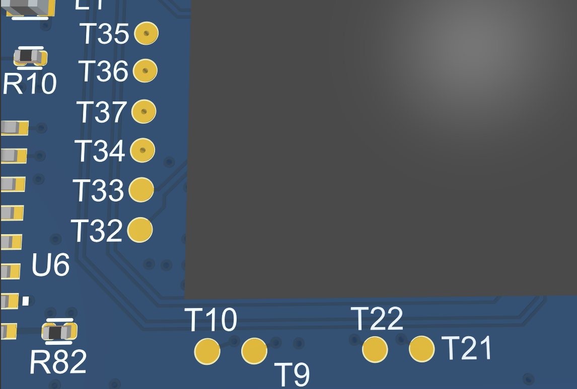
Very simply, printed circuit board test points can be intentionally placed as printed elements in a design, such as a bare pad or a via with a connection to an internal trace/plane. These can then be accessed with a test fixture during electrical testing, such as basic electrical (continuity) testing, in-circuit testing, or a fixture-les flying probe test. Even if you do not intentionally place PCB test points as pads or other fixtures in your PCB layout, you can still define specific conductors as test points.
Does every design need printed circuit board test points? Not necessarily; for a prototype, you’re better off taking the time to do functional testing by hand so that you can more easily identify any failures. You’ll be able to see and touch the boards and instruments you’re working with, so it will be much easier to identify problems during testing. If you’re scaling in any way and you’ve thoroughly evaluated your testing requirements, then it’s best to place PCB test points for in-circuit or functional testing with your manufacturer, this way they can automate those basic functional tests on the line.
As far as test points, they can be placed as components, pads, vias, or other printed elements on your board. Test points can also be tagged for access during fabrication or assembly in your design software. Now, let’s look at some of the options you have for test points in your PCB layout.
Test Point Pads and Vias
One thing you can do is intentionally place a pad along an interconnect or somewhere on a bus as a test point. You could also place this as a via so that inner layers could be easily accessed. These could be placed along a trace (in series) or off to the side as a small stub. For low-speed digital and low-frequency analog (even if it is impedance controlled, this will not be a signal integrity problem. More specialized testing with high-speed/high-frequency signals will need a specific test structure with controlled and matched impedances at each port; keep this in mind before going and placing PCB test points over every interconnect.
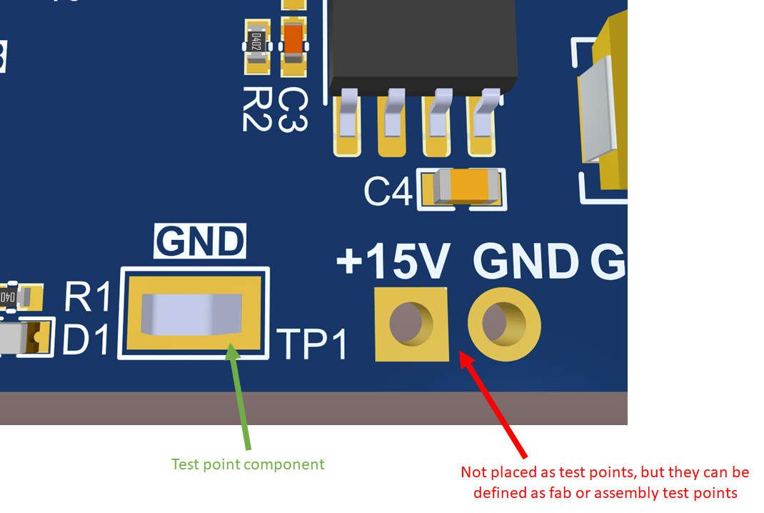
Test Point Components
Some companies manufacture and sell test point components that can be mounted directly on your PCB. An example from Keystone is shown below. This component will be defined in your schematic as a 2-terminal component and placed in the layout just like any other through-hole component. SMD components are also available.

These components are great for attaching a probe to take measurements of a waveform. Note that these only have one connection point. If you’ve connected this test point in series with the target interconnect, you can use this component to measure the voltage waveform on the target interconnect (i.e., with an oscilloscope). At low-to-moderate frequencies (below 1 GHz) and rise times (above 10-20 ns), you can use a direct connection with your probe to take your measurement, and you won’t have to worry about test point impedance or reflections as long as the frequency is low enough. This makes these components good for accessing important waveforms like motor drive, low-frequency analog, slower digital buses (I2C or SPI, for example), or GPIOs on your MCU during functional testing.
Mix and Match
In general, you can mix and match different types of test points depending on your needs. Best practices would dictate placing a test point component or specific test fixture on the board if you need to access an interconnect or waveform during functional testing. Otherwise, for in-circuit testing, flying probe tests, or continuity testing, you should place pads or vias to touch specific points in your board. Test points that aren’t placed as specific pads or fixtures are normally defined on specific vias, component pads, power/GND connections, or other exposed conductors on the fabricated PCB.
More Specialized Testing
What we’ve shown here is intended for in-circuit testing during fabrication/assembly, as well as testing the PCB with a probe to look at a waveform or level. For something more specialized, like a highly accurate impedance measurement or impulse response measurement, simple PCB test points with a simple conductor connection (either mechanically fixed or soldered) might not give you the results you expect. More sophisticated test fixtures are needed to connect your PCB test point access to your signal generator or analyzer. One example is the 2x-thru design as specified in the IEEE P370 standard.
Oftentimes, when a specialized interconnect is being designed for use in a high-frequency or high-speed system, the strategy is to build a test board that holds the interconnect and its connectors. If you specify controlled impedance for your fabricator, they will not test specialized interconnect designs (such as a waveguide) as they won’t have a test coupon that has your specific interconnect. Standard transmission line types are fine, but something more specialized requires you to build the test coupon yourself, or you provide the design files for the test coupon to your PCB fabrication house so that they can test it.
For some low-impedance PDN measurements with short impulses or frequency scans below about 10 GHz, you can just use coaxial connections to test probes that touch your PCB test point pads to make a low-impedance connection. If you’re doing frequency domain measurements to get network parameters, be mindful of error sources related to your reference selection. I’ve covered this elsewhere in regard to power integrity, as have other experts who specialize in low-impedance S-parameter measurements.
When you need to place a PCB test point as a printed element, probe connection, or a specialized test fixture, use the complete set of design features in Altium Designer®. The complete set of test point management tools and the Draftsman utility can help you specify your test point and performance requirements for your product. When you’ve finished your design, and you want to release files to your manufacturer, the Altium 365™ platform makes it easy to collaborate and share your projects.
We have only scratched the surface of what’s possible with Altium Designer on Altium 365. Start your free trial of Altium Designer + Altium 365 today.

About Author
Related Resources


Related Technical Documentation


Table of Contents
Take advantage of the world's
most trusted PCB design system.
One interface. One data
model. Endless possibilities.
Effortlessly collaborate with
mechanical designers.
The world's most trusted
PCB design platform
Best in class interactive
routing
View License Options
Thank you, you are now subscribed to updates.