Ebook: Routing High-Density Interconnects with Reliable Microvias

As electronics have become miniaturized, the technologies used to route interconnects have been pushed to their limits, and new modes of designing PCBs with high reliability have become standard. HDI PCBs take a particular approach to routing interconnects through multiple layers to ensure reliability during fabrication, assembly, and operation. The critical structure that enables this is microvias, which are prone to failure if not designed properly. Some simple design decisions will have a major impact on reliability and solvability in an HDI PCB layout.
In this e-book, readers will receive an initial look at the reasons microvia reliability has come into the spotlight and why HDI PCB designers put reliability first when routing through microvias. Covered topics include:
- Warnings from the IPC regarding reliability of via structures in HDI PCBs
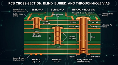
- How to design microvias to ensure reliability
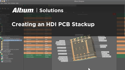
- How to create a PCB stackup for a high density circuit board
- How to set up design rules for layout and routing in HDI PCB design
Click the PDF above to read more about routing in an HDI PCB layout and how to design interconnects for HDI PCBs. You can also read the original, full-length content here:
The IPC Warning About Microvia Reliability for High Performance Products
Everything You Need to Know About Microvias in Printed Circuit Design
Advanced High Density PCB Design in Altium Designer
How to Setup HDI PCB Layout and Routing in Your PCB Design Software

About Author
About Author
Zachariah Peterson has an extensive technical background in academia and industry. He currently provides research, design, and marketing services to companies in the electronics industry. Prior to working in the PCB industry, he taught at Portland State University and conducted research on random laser theory, materials, and stability. His background in scientific research spans topics in nanoparticle lasers, electronic and optoelectronic semiconductor devices, environmental sensors, and stochastics. His work has been published in over a dozen peer-reviewed journals and conference proceedings, and he has written 2500+ technical articles on PCB design for a number of companies. He is a member of IEEE Photonics Society, IEEE Electronics Packaging Society, American Physical Society, and the Printed Circuit Engineering Association (PCEA). He previously served as a voting member on the INCITS Quantum Computing Technical Advisory Committee working on technical standards for quantum electronics, and he currently serves on the IEEE P3186 Working Group focused on Port Interface Representing Photonic Signals Using SPICE-class Circuit Simulators.
Related Resources
Related Technical Documentation
Design to Release, Without the Friction
- Keep reviews tied to the right version
- Reduce handoff confusion and rework
- Spot sourcing and release risk earlier
- Work solo, share when needed
Get Started

PCB Design
Equip engineers with everything needed to design modern, high-performance PCBs.

Product Design
Combine advanced PCB design with cloud-based collaboration to streamline development.


