Transmission Lines in PCB Track Design

Digital designs fall broadly into two categories: low-speed and high-speed. The category “high speed” does not necessarily mean a high clock rate. Rather, it refers to the rise time of the signal during switching, which leads to propagating wave behavior on long PCB tracks. When a PCB track gets too long, it needs to be designed like a transmission line, not just a simple conductor with DC resistance.
Understanding how to design transmission lines with controlled impedance and desired bandwidth is an important skill in high-speed PCB design, but you don’t have to do all of these calculations by hand. Altium Designer includes a range of features to help automate these important tasks in high-speed design, and it’s all accessible inside your standard high-speed routing tools. Keep reading to learn more about routing and signal integrity for transmission lines for high-speed digital PCBs.
ALTIUM DESIGNER®
The industry’s best electronics design platform for transmission line design and analysis in your circuit board.
If it’s your first jump into high-speed design, there are some basic concepts to tackle before creating your first high-speed digital layout. Designing PCB tracks and understanding when they exhibit transmission line behavior are foundational for routing high-speed boards and creating a layout with ensured signal integrity. If your board has signal integrity problems, it may not function properly and will need to be redesigned.
When you need to design your transmission lines and PCB tracks to important low-speed and high-speed specifications, pay attention to these design guidelines. Be sure to use the industry’s best routing tools to help automate your design and layout processes for your high-speed circuit board.
What Goes Into Transmission Lines and PCB Tracks
If you know that your PCB tracks will exhibit transmission line behavior, then the geometry of your PCB tracks needs to be carefully designed so that your tracks have the specific impedance value as defined in your high-speed signaling standard. In addition to impedance, crosstalk and losses need to be kept in the PCB layout to ensure signal integrity during operation. The cross-sectional geometry of your PCB tracks, the track length, and layer stackup will affect all of these areas.
The important parameters that determine the impedance of your PCB tracks are:
- Track width
- Copper weight (track thickness)
- Distance to the nearest plane layer
- Dielectric constant and magnetic permeability of the PCB substrate material
Each of these parameters needs to be carefully chosen to ensure signals on transmission lines in your PCB see the correct impedance. The goal is to prevent signal integrity problems that arise when traces do not have correct impedance, are too long, or couple too much noise.
Design Your PCB Layer Stack to Prevent Signal Integrity Problems
Preventing signal integrity problems that happen on incorrectly designed transmission lines starts with designing the correct stackup. Your PCB layer stack will contain the arrangement of plane and signal layers in your PCB, and a ground plane placed below your PCB tracks will determine their impedance, coupling strength to other traces, and immunity to EMI.
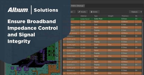
Altium Designer’s layer stack manager lets you design your stackup so that you set the required impedance for your transmission lines. You won’t have to use an external field solver to determine the trace geometry that gives you controlled impedance, everything you need can be found in Altium Designer.
- Your PCB tracks will act like transmission lines once the track length is longer than a critical length.
Learn more about the critical length in transmission lines on your PCB.
- All PCB substrates exhibit dispersion that needs to be considered when designing transmission lines for your circuit board layout.
Learn more about dispersion and how it affects digital signals in your PCB layout.
- The layer stack manager in Altium Designer helps you design your PCB tracks to have specific impedance. Once your PCB tracks are routed over a long enough distance, Altium Designer ensures your transmission lines will have the required impedance.
Learn more about using the layer stack manager in Altium Designer for impedance control.

Altium Designer makes it easy to design transmission lines with specific impedance values.
Routing and Length Matching in High-Speed PCB Designs
Once your PCB transmission lines have been designed with the right geometry and impedance, you need to use this design to define printed traces between components on your circuit board. High-speed PCB traces need to be routed with the specified width to ensure impedance control, but groups of traces may also need to be length matched to ensure that signals arrive at their destination within a required unit time interval.
The best routing tools will enforce width and length constraints on your transmission lines automatically. You won’t have to manually measure transmission line lengths or set trace widths as you route signals across your board. Instead of checking and applying these constraints manually, use the best set of routing features that interface directly with your impedance-controlled transmission line design.
Altium Designer Includes the Best Set of Routing Features for High-Speed PCBs
Impedance-controlled routing and length matching are easy in Altium Designer’s best-in-class high-speed PCB design tools. The routing engine in Altium Designer takes information directly from your PCB layer stack to define trace widths, and length tuning can be applied in your board automatically during routing. Only Altium Designer provides these features alongside your other design tools, helping you stay productive as you create advanced circuit board layouts.
- Underwater ROV boards can be ceramics or metal-core PCBs, which will ensure high reliability and mechanical stability during operation.
Learn more about designing circuit boards from exotic materials.
- Your board needs to be designed to comply with important DFM rules to ensure it can be put into standard PCB manufacturing processes.
- Routing transmission lines correctly will help prevent crosstalk between signals in your high-speed PCB layout.
See an example of crosstalk and coupling on high-speed DDR4 lines in an Altium Designer PCB layout.

Dense layouts with high-speed signals will have long traces that couple noise to each other. Altium Designer includes the stackup design and routing tools you need to ensure signal integrity.
Use Design Rules to Evaluate Your Layout
Before you can prepare your board for manufacturing, it’s best to check your PCB layout against your design rules to ensure no errors exist that might cause signal integrity problems. Although the best routing tools will apply transmission line design constraints to your tracks as you create your PCB layout, it’s best to check the entire layout for clearances, hole and track sizes, component collisions, and other electrical constraints.
Altium Designer gives you these rules-driven design capabilities and much more. Rules-driven design software with an online DRC engine will run these checks for you as you create your PCB layout. It’s easy to spot, fix, and prevent errors in your circuit board designs as you create your layout.
Comprehensive Design and Manufacturing Features in Altium Designer
Once your design is finished, Altium Designer’s complete set of circuit board design features will help you quickly generate documentation for your manufacturer. Instead of using 3rd party software, Altium Designer will take data directly from your PCB layout and generate your manufacturing deliverables automatically. No other PCB design software platform makes it this easy to put a new design into full-scale production.
- Altium Designer’s rules-driven design engine unifies all your design and layout features in a single program and helps you stay productive.
- The newest version of Altium Designer includes an integrated field solver that ensures your transmission line designs will have the correct impedance.
Learn more about Simberian’s integrated field solver in Altium Designer.
- You can store, share, and access your high-speed design data with the Altium 365 platform, the industry’s only cloud-based platform for PCB design collaboration.
Learn more about managing and sharing design data with Altium 365.

Create your high-speed PCBs with the complete set of design features in Altium Designer
When you need to design transmission lines and PCB tracks for any electronics application, use the industry’s best set of layout, routing, sourcing, and fabrication features. You’ll find all of these critical circuit board design features and much more when you make the switch to Altium Designer.
Altium Designer on Altium 365 delivers unprecedented integration to the electronics industry until now relegated to the world of software development, allowing designers to work from home and reach unprecedented levels of efficiency.
We have only scratched the surface of what is possible to do with Altium Designer on Altium 365. You can check the product page for a more in-depth feature description or one of the On-Demand Webinars.


