

New Customers Only. Offer Expires Feb 28, 2025
Up to 30% Off Altium Designer!
Interested? Call: 1-800-544-4186 , Email: sales.na@altium.com
New Customers Only. Offer Expires Feb 28, 2025
Which BGA Pad and Fanout Strategy is Right for Your PCB?

Many advanced components are placed in BGA packages, ranging from large processors to memories and even small audio chips. These packages require a fanout and escape routing strategy to reach the pads beneath the component, and routing into the component might require controlled impedance. If this describes a component you're working with, then you'll need to consider multiple points to correctly route into a BGA.
In this article, I'll look at the fanout strategy you'll need to route into a BGA and when the ball pitch will become too small to use traditional dog bone fanout. When the land pattern gets small enough, you will make a shift to via-in-pad, and eventually to laser drilled vias and into the HDI realm.
BGA Fanout Options
The term "fanout" in PCB design and routing refers to the breaking out pads routing channels from the land pattern for your BGA component. There are two principle methods for breaking out routing channels below a BGA:
- Dog bone fanout
- Via-in-pad
At large pitch, you can use dog-bone fanout, while via-in-pad is needed at smaller pitch. The dividing line between "large" and "small" in reference to ball pitch is not cut and dry; it depends on the required trace width coming into the BGA. The trace width coming into the BGA then depends on the need for controlled impedance, which is calculated from the dielectric thickness and dielectric constant.
There is another fanout style related to dog bone fanout, where smaller pads are broken out at sub-45 degree angles. This is seen in mid-range pitch BGAs (between 0.5 and 1 mm ball pitch) but is not necessarily required. If you can master the core concepts in dog bone and via-in-pad fanout and escape routing, you can also master other fanout strategies that deviate from these standard options.
Dog Bone Fanout
The image below shows how a dog bone fanout is placed below a BGA. In this image, the outer 2 row/column groups of pads can be used for directly routing into the BGA landing pads. The remaining pads on inner rows/columns will need to be accessed through an internal layer through the vias. The vias are then connected back to the solder pads on the BGA. Technically, dog bone could be used for any BGA pitch, but practically this will be used when the BGA pitch is larger than 0.5 mm to 0.75 mm.
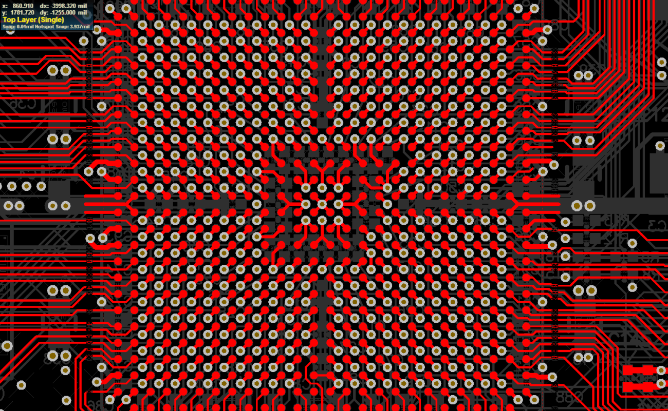
To get between the pads in a dog bone fanout, the trace needs to be thin enough to pass between pads without violating clearance limits between copper elements. The clearance limit between copper elements is based on manufacturability and fabrication tolerances.
So, how wide should the trace be? Consider the situation below, where a trace is being routed between two copper pads; these could be the BGA pads on the outer two rows/columns on the top layer, or non-functional pads on vias in an inner layer. The trace with width W is being routed between these two elements for a given pad diameter D and spacing d.

There will be some fabrication limit f that must not be exceeded, so we must satisfy the condition d > f. You can use this to solve for an upper limit on the trace width:

This result makes sense: larger pitch allows larger widths, but larger fabrication limit and larger pad diameter force you to use smaller trace width. You can use this value to determine the dielectric thickness you should use in the PCB stackup. If the interface you're reaching is not impedance-controlled, then just size the trace to the width you need to get between those pads/vias. In the internal layers you might need to remove non-functional pads on inner layers to get traces between the vias in the fanout pattern.
When to Shift to Via-in-Pad
This question is totally divorced from designing the footprint and it is based on whether you can fit pads between balls in a dog bone fanout. When ball density becomes so high that the pad pitch gets closer to 0.5 mm, dog bone fanout can no longer be used unless the drill size is reduced, sometimes below 8 mils. The exact transition limit depends on the smallest drill size that can be used and the pad size that is required, such as with Class 2 or Class 3 compliance for annular rings.
In the fine-pitch case, BGA pads can connect to the inner signal layers using via-in-pad technology, and the trace width calculation above still applies. If BGA pads are placed directly on vias, the vias will be filled and plated over in order to prevent the solder ball from wicking into the via. The best practice is to fill those vias to ensure the strongest bond between the plating and the interior of the via, either with conductive or non-conductive epoxy. If high reliability is required, check with your fabricator to see which type of fill they recommend for your particular operating conditions.
SMD vs. NSMD BGA Pads
The landing pads for the BGA must be designed as a function of the pitch, and they must be designed with the correct solder mask opening. When designing a land pattern, some minimum amount of copper should be exposed to ensure acceptable solder accumulates and bonds on each landing pad below the BGA. There is a rule of thumb that says to set the copper pad diameter to about 80% of the BGA ball size, but the linked article below provides more specific numbers on exactly how large BGA pad sizes should be.
There are two types of pads that can be used to design BGA land patterns for your PCB. The solder mask defined (SMD) pad coats the edge of the pad with a small amount of solder mask. This effectively reduces the exposed pad size in your BGA land pattern, and it forces the solder ball to sit atop the pad. This thin ring of solder mask elevates tends to elevate the solder ball so that its curvature sits slightly above the solder resist.
There are two other advantages of using SMD pads:
- The opening in the mask creates a channel for each ball on the BGA to align with while the pad during soldering
- The overlapping mask helps prevent the pads from lifting off the PCB due to thermal or mechanical stress.
Both are useful from a reliability perspective. These pads are just fine for larger-pitch BGAs as long as there is plenty of space for routing. If you sized the trace correctly based on the dielectric thickness, then you can route between the balls on the BGA even with SMD pads. Contrast this with the non-solder mask defined (NSMD) pad. NSMD pads expose the entire copper area in the pad for soldering. In other words, the solder mask opening is at least as large as the pad, and it could be larger. Always check your component datasheets before placing either type of BGA pad in your PCB layout.
Once you've defined the fanout, escape routing will be used to connect the BGA pads to external traces, which in turn connect to other components on the PCB. Routing out of the BGA will generally require multiple layers in order to fit all of the required traces. One PCB layer is sufficient to route a two row thick square at the edge of the BGA. The next two row square deeper into the BGA requires its own signal layer. As you continue to move into the BGA, this pattern repeats, and more signal layers must be added to the PCB.
In BGA with high pin count and fine pitch, the trace width may need to be adjusted as you route into BGAs. This technique is called “necking” or "neck-down," where the trace width is reduced coming into the BGA. This change in width mid-trace creates a characteristic impedance discontinuity unless the trace neck-down is perfectly sized as an RF taper. In low-speed or low-frequency devices, the input impedance along that neck-down region will probably be negligible if the traces are short enough. This is one reason that some BGAs will place controlled impedance interfaces around the edge of the BGA footprint; that way necking can be avoided.
Note that, if you need controlled impedance, then you should focus on selecting the stackup materials such that the resulting trace width is small enough that necking is not needed coming into the BGA. I'll soon publish another article on this as the material stackup is not always selected such that high-speed routing into a BGA can be accommodated.
When you need to place BGAs in your PCB layout, define a fanout, and create an escape routing strategy, use the complete set of PCB design tools in Altium Designer®. When you’ve finished your design, and you want to release files to your manufacturer, the Altium 365™ platform makes it easy to collaborate and share your projects.
We have only scratched the surface of what’s possible with Altium Designer on Altium 365. Start your free trial of Altium Designer + Altium 365 today.











 Back
Back