Microstrip Patch Antenna Calculator for RF Designers
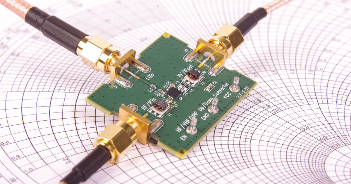
Microstrip patch antennas and arrays are probably the simplest antennas to design next to monopole and dipole antennas. These antennas are also easy to integrate into a PCB, so much so that they are commonly used in advanced systems like 5G antenna arrays and radars. These antenna arrays also follow a simple set of design equations in the fundamental mode and in higher order modes, so you can even design them without using a simulation tool.
In this article, we’ll present the main equations used to design a microstrip patch antenna that provides operation in a fundamental mode, and that allows extension into higher order modes. We’ll also provide a lightweight microstrip patch antenna calculator application that can be used to size a patch antenna given a substrate thickness, Dk value, and operating frequency.
How Microstrip Patch Antennas Work
Microstrip patch antennas are essentially open resonators. The antenna is placed above a ground plane, and field confinement between the patch antenna and the ground plane determines a set of eigenmodes in which the antenna can operate (similar to non-TEM transmission lines). The eigenmodes correspond to specific modal field distributions inside the resonant cavity created by the antenna, although these antennas are typically operated in the fundamental mode. An illustration of the field distribution around a patch antenna on a PCB is shown below.

Because this is an open resonant structure, it can radiate strongly when a mode is excited. Just like other resonant structures, the frequency of operation is easily tuned by adjusting the length and width of the patch antenna, as well as the height above the ground plane. The input impedance is then equal to the ratio of the electric and magnetic fields around the patch antenna.
Microstrip Patch Antenna Design Equations
The design of a microstrip patch antenna relies on the following equations. First, we have an effective dielectric constant for a given PCB substrate Dk value, which then determines the width and length of the patch for a given operating frequency. The design process goes as follows:
- Select an operating frequency (f0)
- Calculate the patch width (W) using the substrate dielectric constant (Dk) and thickness (h)
- Calculate an effective dielectric constant
- Calculate the patch length (L) using results from Steps 2 and 3; this completes the design problem

When higher order mode operation is desired, the width, length, and frequency must satisfy the following equation:

Note that the L* term refers to L above, plus the 2nd term on the right hand side:

The main set of design equations for L and W assume we are operating in the (i, j, k) = (1, 0, 0) mode. The next highest order frequency involving L* determines a cutoff for the patch antenna due to its excitation from the edge.
By substituting the above equation for L into this equation, you can get a more complex equation relating frequency and W with h as a parameter. This can then be solved by hand, by graphing intersections, or using a random search application like differential evolution.
Input Impedance and Bandwidth
As I mentioned above, the input impedance looking into the antenna is equal to the ratio of the electric and magnetic fields. In the fundamental mode, the fields are nearly constant along the feedline width right at the edge, and the input impedance looking into the antenna is given by:

Microstrip patch antenna input impedance in the fundamental mode (i, j, k) = (1, 0, 0).
Finally, there is a bandwidth that can be defined in the frequency domain (units of Hz). Note that this defines the bandwidth given the operating frequency and wavelength in free space:

A Microstrip Patch Antenna Calculator
The calculator tool shown below will provide input impedance and the dimensions of a microstrip patch antenna given a desired operating frequency, substrate dielectric constant (Dk), and distance to the reference plane through the substrate (h).
Next Steps
Once the input impedance is known, the designer will need to match the input impedance at the feedline connection to the patch. Typical guides show the use of a quarter-wave impedance transformer, but these feedline sections will be comparable to the size of the antenna, so this might make the system unnecessarily large.
Because these patch antennas can have moderate Q-values, they can radiate efficiently over bandwidths up to about 10% of the carrier frequency as long as impedance transformers are not used for impedance matching. For broadband matching with bandpass filtering, a higher-order LC filter may be needed; this will be a topic for a future article.
Microstrip Antenna Inset Feed Calculator
One option for impedance matching is to use an inset, as shown in the image below. The line inset is designed to set the input impedance looking into the edge of the patch to a target impedance. This works by taking advantage of coplanarity between the antenna and the feedline, which produces some capacitance along the input section of the feedline. The feedline dimensions are shown below:

The inset feedline design relies on the equation below, which is used to determine the depth of the inset into the antenna patch. The inputs are a target input impedance, which will be equal to the impedance of the feedline into the patch antenna (typically 50 Ohms). The feedline will reach a certain depth into the antenna, and the depth to spacing ratio (D/S) will affect the input impedance. The required design equation relating the inset depth, antenna impedance, and feedline impedance is:

Note that there is a cos^4 dependence, which is contrary to most microstrip antenna inset calculators. Most calculators will list a cos^2 dependence, but this is a point of confusion as the cos^2 dependence applies to a probe-fed antenna. It only applies to an inset-fed antenna when D/L is large.
The design concept is simple and follows this process:
- The feedline width required for a target impedance (generally 50 Ohms) is determined
- This impedance is used to calculate the depth (D) into the patch antenna
- The spacing (S) is determined
The calculator below provides an inset feedline distance for a given antenna impedance and feedline impedance.
Here we’ve calculated the input distance, but not the spacing. This is because the spacing is much more difficult to predict and requires interpolation from measurement or a field solver. The graph below shows the cosine-dependence of the input impedance as a function of D/L with S as a parameter. We can see that there is a universal result where the spacing is between S = (1 to 2)W0 for an inset distance of approximately 0.25L, giving a target input impedance of 50 Ohms.

The above graph can be found in an excellent publication outlining the theory and implementation of patch antennas:
When To Use Microstrip Patch Antennas
These antennas are very easy to design and implement, but they are also limited in their usage by available board area. Microstrip patches can be rather large because they rely on resonant excitation between the patch and the reference plane. This means that the microstrip patch size will be proportional to the wavelength of the signal that is being broadcast/received by the antenna.
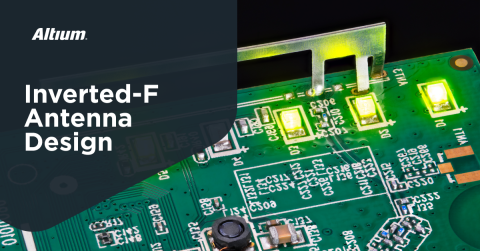
A smaller alternative may be a printed microstrip antenna, such as a printed trace antenna or an inverted F antenna. The inverted-F is used in some popular MCU boards or modules, for example the ESP32 Ai-Thinker module shown below.

Finally, I’d like to point out that microstrip patch antennas are the primary type of antenna being used in more advanced commercial applications. Two prominent examples are radar (short and long range) and 5G (reaching into the mmWave range). In radar, patch antennas are being used in series-fed patch arrays used in phased arrays. The main reason for this is their size is much smaller at higher frequencies found in mmWave bands. In 5G, these patches are used because they can be used in an array with a transceiver on the back side of a PCB or package, so it is possible to form very dense antenna arrays.
The CAD features in Altium Develop are ideal for any type of design you want to create, ranging from high-speed digital PCBs to advanced RF systems. When you’ve finished your design, and you want to release files to your manufacturer, Altium Develop makes it easy to collaborate and share your projects.
Whether you need to build reliable power electronics or advanced digital systems, Altium Develop unites every discipline into one collaborative force. Free from silos. Free from limits. It’s where engineers, designers, and innovators work as one to co-create without constraints. Experience Altium Develop today!

