How to Calculate Impedance-Controlled Routing In Your PCB And Design Rules


In high-speed PCB design, many standard interfaces are impedance-controlled, meaning the trace connecting to a chip must have a specific impedance value. This article is not necessarily about calculators or formulas for calculating impedance, but rather how and when to use the calculation in a stackup design process. PCB stackups can be custom designed, selected from a standard stackup, or there may not be any data given to you at the beginning of the design.
What should you do in each of these cases? This article will give an overview of the process for each of these potential situations as well as what you can expect from your PCB fabrication company.
It Starts with Your PCB Layer Stackup
Once your circuit designs are complete and the main components are selected, the time to start planning your impedance-controlled routing is when you are creating the PCB stackup. Generally, you will start with a target impedance value, and you want to calculate the trace size for a given stackup. There are a few ways to approach trace sizing, depending on the stackup you intend to use and how you want to design or approach the stackup.
The table below briefly lists some approaches to trace sizing and dielectric thickness sizing as part of calculating impedance-controlled routing. Each entry in the table starts by assuming one of the parameters in the design is known, and the other must be determined.
|
Start with |
You calculate |
|
|
Controlled impedance |
Trace width |
Impedance target |
|
Controlled dielectric |
Impedance target |
Trace width |
|
Standard stackup |
Either impedance target or trace width |
|
In short, if you have a trace width target and no other hard requirements (such as HDI or loss budget), then controlled dielectric is often a simple approach. If there are many hard requirements you need to balance, then controlled dielectric is normally the best approach. A middle ground where you can still have some flexibility and possibly access more advanced requirements, such as low loss tangent and HDI buildup, is by using standard stackups, although the stackups available vary greatly among different fabricators.
Controlled Impedance Calculation
In the controlled impedance approach, you aren't calculating anything. Essentially, you get to choose the trace width that you want, or the width and spacing for differential pairs. Once you have selected these values and sent the design off to a fabrication house, the fabricator will mix and match their materials to hit your target impedance. They will need to test the impedance during fabrication using a TDR with some test traces on a breakaway rail. This is the most common approach that is referred to as "controlled impedance," despite the fact that the designer is not directly calculating any impedance values.
To communicate this to your fabrication house, you will need to include a table with trace widths and corresponding target impedance values for different layers. Construction of this table is a bit of an art, particularly when multiple interfaces with different impedances are placed on the same layer.

Depending on the trace width you specify, the fabricator might inform you that this forces layer thicknesses to be too thin or too thick. For example, if you specify a microstrip trace width that is large but also require blind vias, the resulting large dielectric thickness could force your blind via aspect ratio to also be quite large. Conversely, if you specify a narrow microstrip trace, this may force you to use very thin dielectrics, which could create higher costs. It's best to have some understanding of these other issues, as well as an estimate of typical layer thicknesses, before you begin specifying trace sizes.
Standard Stackup Calculation
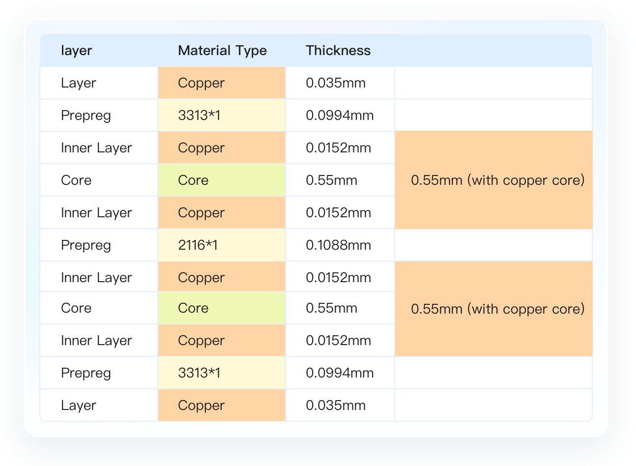
With the standard stackup approach, the fabricator gives you a stackup construction, which will be complete with dielectric constant values and layer thickness values.
For example, many designers who have used JLCPCB are likely aware that they provide several standard stackup options for different layer counts.

The dielectric constant and thickness values could be programmed into the stackup manager in your PCB design software and used to calculate the impedance of your traces. In Altium Designer, you would enter this information into the Layer Stack Manager inside your .PcbDoc file. Then, using the impedance solver in the Layer Stack Manager (controlled dielectric approach), the solver will generate the width that hits your required impedance targets.
Controlled Dielectric Calculation
As mentioned above, "controlled impedance" could actually refer to controlled dielectric, the former of which does not require an impedance calculation by the designer. Taking the controlled dielectric approach refers to designing your own stackup from commercially available materials and calculating trace impedance values within your stackup design.
This approach is not for new designers because it requires some knowledge of material availability, or at least of material vendors, so that you can inquire about their material offerings. Whether you already know of a specific material or need to contact a vendor to get material offerings, your job will be to place the material thickness and dielectric constant values for each layer into your PCB stackup editor. In Altium Designer, you would also use the Layer Stack Manager, as mentioned above in the standard stackup section.
Make sure the laminate product names you select for each layer are specified and included in the layer stack. This can be done by editing the entry in the "Material" column in Altium Designer's Layer Stack Manager window.
An important point here is that this approach gives you full control over the broadest aspects of your design. For example, HDI design and via sizing, advanced material selection, and non-symmetric or hybrid stackup options are all possible when the designer is specifying the layers in the PCB stackup. There are many fabrication houses that can't or won't provide this service, so for more advanced products, it becomes the designer's responsibility to make those determinations.
When you create your fabrication documentation, you can then generate a stackup table that shows the laminate product name for each layer. This can be done in Draftsman using the built-in tools, so there is no need to manually draw out stackup tables to specify your PCB construction.

Executing an Impedance Calculation
Whenever you need to calculate trace impedance or differential impedance, the task is very straightforward:
- Single-ended trace: Calculate the width needed to hit the impedance target, or vice versa.
- Differential traces: Calculate the width for a chosen spacing needed to hit the impedance target, or vice versa for a set width and spacing.
These tasks are easily accomplished in the Layer Stack Manager inside Altium Designer, thanks to the integrated field solver from Simbeor. This solver tool uses cutting-edge 2D models that calculate the quasi-TEM transmission line impedance in single-ended and differential configurations.
Once an impedance profile is created, it can be applied as a design rule under the Routing -> Width section of the PCB Rules and Constraints Editor. From here, you can select one of your impedance profiles and set the rule's scope to a specific net, net class, differential pair, or differential pair class. The PCB editor will then automatically check your routing against this impedance profile as you create your PCB layout.
Whether you need to build reliable power electronics or advanced digital systems, use the complete set of PCB design features and world-class CAD tools in Altium Designer®. To implement collaboration in today’s cross-disciplinary environment, innovative companies are using the Altium 365™ platform to easily share design data and put projects into manufacturing.
We have only scratched the surface of what’s possible with Altium Designer on Altium 365. Start your free trial of Altium Designer + Altium 365 today.


