


Top 5 PCB Design Layout Guidelines You Need to Know

At a Glance
We've compiled some of the essential PCB layout guidelines every designer should know to ensure your board will work as intended. Written by a leading industry expert.


Whether you are moving at a high speed or you're designing a high-speed printed circuit board, good board design practices help ensure your design will work as intended and can be manufactured at volume. In this guide, we've compiled some of the essential PCB board design and layout guidelines that apply to most modern circuit boards. Specialty designs may need to follow additional board layout guidelines, but the PCB design and layout guidelines shown here are a good place to start for most board designs.
The PCB design guidelines shown here are focused on a few key areas that will help you with routing, manufacturability, basic signal integrity, and assembly:
- Defining PCB design rules with the goal of ensuring fabrication and assembly yield
- Component placement, where the goal is to ensure solvability and ease of routing
- Grouping components by type to prevent the need to route all over the board
- Location of power and ground in the PCB stack-up, including some points for mixed signal PCB layout designs
- Obeying mechanical constraints, such as connector locations and enclosure limitations
#1 - Determine Your PCB Board Design Rules Before Layout
When starting a new printed circuit board design, it’s sometimes easy to forget about the important PCB design rules that will govern your project. There are some simple clearances that, if determined early in the design, will eliminate a lot of component shifting and re-routing later. So where can you get this information?
The first step is to talk to your PCB design rules fabrication house. A good fabricator will usually post their capabilities online or will supply this information in a document. If it's not in an obvious location on their website, send them an email and ask for their capabilities. It's best to do this first before you start placing components. While you're at it, make sure to submit your proposed stack-up for review or look for their standard stack-up data and use that.
Once you've found their list of capabilities, you should compare these to whatever industry reliability standard you'll work with (Class 2 vs. Class 3 or a specialty standard). Once these points are determined, you should select the more conservative design layout limits needed to ensure manufacturability and reliability, and you can encode these into your PCB design rules.
As you proceed through the layout process, your PCB design rules will help you eliminate most design errors that will lead to fabrication and assembly problems. After setting the board design rules, you can start the placement process.
#2 - Fine-Tuning Your Component Placement
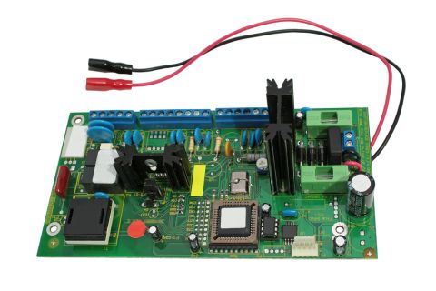
The component placement stage of your PCB layout design process is both an art and a science, requiring a strategic consideration of the prime real estate available on your board. The goal in component placement is to create a board that can easily be routed, ideally with as few-layer transitions as possible. In addition, the design has to comply with the PCB design rules and satisfy must-have component placements. These points can be difficult to balance, but a simple process can help a board designer place components that meet these requirements:
- Place must-have components first. There are often components that must be placed in specific locations, sometimes due to mechanical enclosure constraints or due to their size. It's best to place these components first and lock in their position before proceeding to the rest of the layout.
- Place large processors and ICs. Components like high pin count ICs or processors generally need to make connections to multiple components in the design. Locating these components centrally makes trace routing easier in the PCB layout.
- Try to avoid crossing nets. When components are placed in the PCB layout, the unrouted nets are normally visible. It's best to try and minimize the number of crossing nets. Each net intersection will require a layer transition through vias. If you can eliminate net crossings with creative component placement, it will be easier to implement the best routing guidelines for a PCB layout.
- SMD PCB board design rules. It’s recommended to place all surface mount device (SMD) components on the same side of the board. The main reason for this arises during assembly; each side of the board will require its own pass down the SMD soldering line, so placing all SMDs on one side will help you avoid some extra assembly costs.
- Experiment with orientation. It's okay to rotate components to try and eliminate net intersections. Try to orient connected pads so that they face each other, as this can help simplify routing.
If you follow points #1 and #2, it's much easier to lay out the rest of your board without too much crossover between routes. In addition, your board will have that modern look and feel to the layout, where a central processor supplies data to all the other components around the perimeter of a board.

#3 - Placing Your Power, Ground & Signal Traces
With components placed, it’s now time to route power, ground, and signal traces to ensure signals have a clean and trouble-free path of travel. Here are some PCB design guidelines to keep in mind for this stage of your layout process:
Where to Place Power and Ground Planes
It’s generally the case that power and ground are placed on two internal layers. For a 2-layer board, this might not be so easy, so you would want to place a large ground plane on one layer and then route signals and power traces on the other layer. With 4-layer circuit board stack-ups and higher layer counts, you should use ground planes instead of trying to route ground traces. For components that need direct power connections, it’s recommended to use common rails for each supply if a power plane is not used; ensure you have wide enough traces (100 mils is fine for 5 to 10 A), and don't daisy chain power lines from part to part.
Some recommendations state that plane layer placement must be symmetrical, but this is not strictly required for manufacturing. In large boards, this might be needed to reduce the chances of warping, but this is not a concern in smaller boards. Focus on access to power and ground, as well as ensuring all traces have strong return path coupling to the nearest ground plane first, then worry about perfect symmetry in the PCB design stack-up.
Routing Guidelines for PCB Layouts
Next up, connect your signal traces to match the nets in your schematic. PCB layout best practices recommend that you always place short, direct traces between components when possible, although this may not always be practical on larger boards. If your component placement forces horizontal trace routing on one side of the board, then always route traces vertically on the opposite side. This is one of many important 2-layer PCB board design rules.
Printed circuit board design rules and PCB layout guidelines become more complex as the number of layers in your stack-up increases. Your routing strategy will require alternating horizontal and vertical traces in alternating layers unless you separate each signal layer with a reference plane. In very complex boards for specialized applications, many of the commonly-touted PCB best practices may no longer apply, and you'll need to follow PCB board design guidelines that are particular to your application.
Defining Trace Widths
PCB layout designs use traces to connect components, but how wide should these traces be? The required trace width for different nets depends on three possible factors:
- Manufacturability. Traces cannot be too thin, otherwise, they can't be reliably manufactured. In the majority of cases, you'll be working with trace widths that are much larger than the minimum value your fabricator can produce.
- Current. The current carried in a trace will determine the minimum required width to prevent the trace from overheating. When the current is higher, the trace will need to be wider.
- Impedance. High-speed digital signals or RF signals will need to have a specific trace width to hit a required impedance value. This doesn't apply to all signals or nets, so you don't need to enforce impedance control on every net in your board design rules.
For traces that don't need specific impedance or high current, a 10 mil trace width is fine for the vast majority of low-current analog and digital signals. Printed circuit board traces that carry more than 0.3 A may need to be wider. To check this, you can use the IPC-2152 nomograph to determine your PCB design trace width for a required current capacity and temperature rise limit.
Preferred routing (arrows indicate component shifting direction)
Non-preferred routing (arrows indicate component shifting direction)
Thermal Relief Connections to Planes for Through-Hole Components
The ground plane can act as a large heat sink that then transports heat evenly throughout the board. Therefore, if a particular via is connected to a ground plane, omitting the thermal relief pads on that via will allow heat to conduct to the ground plane. This is preferable to keeping heat trapped near the surface. However, this can create a problem if through-hole components are assembled on the board using wave soldering, as you need to keep heat trapped near the surface.
Thermal reliefs are one PCB layout design feature that might be needed to ensure a board will be manufacturable in a wave soldering process, or in other words, for through-hole components connected directly to planes. Because it can be difficult to maintain process temperatures when a through-hole is a solder point directly to a plane, it’s recommended thermal reliefs be used to ensure the soldering temperature can be maintained. The idea behind thermal relief is simple: it slows the rate at which heat is dissipated into the plane during soldering, which will help prevent cold joints.
The typical thermal relief pattern
Some designers will tell you to use a thermal relief pattern for any via or hole that is connected to an internal ground or power plane, even if it is just a small polygon. This advice is often overgeneralized. The need for a thermal via on any through-hole component will depend on the size of the copper plane or polygon that will make a connection on the internal layer, and it is something you should request your fabricator review before you place your board into production.
What About Thermals on Copper Pours?
Through-hole pads on copper pour could require the same thermal pad application as planes. When the pour is very large, it starts to look a lot like a plane, and so a thermal pad should naturally be applied if a through-hole pin will be soldered into that connection.
For SMD parts, this is not always the case. Whether the thermal gets applied to the pour region depends on how the PCB will be assembled. A reflow soldering process will heat up the board uniformly as the device passes through the reflow oven, so the potential form tombstoning is much lower for those SMD pads, regardless of the presence of a thermal connection.
If the design is assembled by hand, such as with solder paste and a heat gun, then the PCB layout might need thermals to trap enough heat near the pad and prevent tombstoning. When soldering by hand, it can be difficult to maintain consistent heating across the component leads, and a thermal connection can help prevent a tombstoning defect.

Thermal connection on a polygon in Altium Designer within Altium Develop.
By default, Altium Designer within Altium Develop will maintain thermal connections onto polygons when you create a new project. This is configured using the Polygon Connect rule in the PCB design rules editor. You can change this setting to apply based on specific footprints, layers, component classes, nets/net classes, or any other conditions using the query language in Altium Designer.
#4 - Keeping Things Separate
There are some routing guidelines for PCB design rules about how to group and separate components and traces so that you ensure easy routing while preventing electrical interference. These grouping guidelines can also help with thermal management as you might need to separate high-power components.
Grouping Components
Some components are best placed in the PCB layout design by grouping them in one area. The reason is that they might be part of a circuit and they may only connect to each other, so there would be no need to place the components on different sides or areas of the board. PCB layout then becomes an exercise in designing and laying out individual groups of circuitry so that they can be easily connected together with traces.
In many layouts, you'll have some analog and some digital components, and you should prevent the digital components from interfering with the analog components. The way this was done decades ago was to split up ground and power planes into different regions, but this is not a valid design choice in modern board designs. Unfortunately, this is still communicated in many PCB layout guidelines, and it leads to many bad routing practices that create EMI.
Instead, use a complete ground plane below your components, and do not physically break the ground plane up into sections. Keep the analog components with other analog components operating at the same frequency. Also, keep the digital components with other digital components. You can visualize this as having each type of component occupying a different region above the ground plane in the PCB layout design, but the ground plane should stay uniform in the majority of board designs.
Example of digital & analog sections in a PCB.
Separating High-Power Components
It is also appropriate to separate components that will dissipate a lot of heat on the board into different areas. The idea behind separating these high-power components is to equalize the temperature around the PCB layout rather than create large hotspots in the layout where high-temperature components are grouped. This can be accomplished by first finding the “thermal resistance” ratings in your component’s datasheet and calculating the temperature rise from the estimated heat dissipation. Heatsinks and cooling fans can be added to keep component temperatures down. You may have to carefully balance the placement of these components against keeping trace lengths short as you devise a routing strategy, which can be challenging.
#5 - Rounding Out Your PCB Board Design & Layout
It’s easy to get overwhelmed toward the end of your design project as you scramble to fit your remaining pieces together for manufacturing. Double and triple-checking your work for any errors at this stage can mean the difference between a manufacturing success or failure.
To help with this quality control process, it’s always recommended to start with your Electrical Rules Check (ERC) and Design Rules Check (DRC) to verify you’ve met all of your established constraints. With these two systems, you can easily define gap widths, trace widths, common manufacturing constraints, high-speed electrical requirements, and other physical requirements for your particular application. This automates a review process for validating your PCB layout.
Note that many design processes state that you should run PCB design rule checks at the end of the board design phase while preparing for manufacturing. If you use the right design software, you can run checks throughout the design process, which allows you to identify design potential problems early and correct them quickly. When your final ERC and DRC have produced error-free results, it’s then recommended to check the routing of every signal and confirm that you haven’t missed anything by running through your schematic one wire at a time.
There you have it - our top PCB layout guidelines that apply to most circuit board designs! Although the list of recommendations is short, this guideline can help you get well on your way toward designing a functional, manufacturable board in no time. These PCB board design guidelines only scratch the surface, but they form a foundation for building upon and solidifying a practice of continual improvement in all your design practices.
If you want to get started with the best PCB board design software with a built-in rules-driven design engine that helps you stay accurate, use the advanced design tools in Altium Develop. When a design is finished and ready to be released to manufacturing, Altium Develop makes it easy to collaborate and share your projects. Experience Altium Develop today!
Altium's PCB Layout Capabilities
PCB Layout Documentation
PCB Component Placement
Route Your Most Complex Boards Faster
How to Create a PCB Layout from a Schematic
PCB Design and Development
Top 5 PCB Design Rules
Board Layout with Altium
PCB Layout and Placement Guidelines
Rules-Based Component Placement

About Author
Related Resources
Related Technical Documentation
Table of Contents
Design to Release, Without the Friction
- Keep reviews tied to the right version
- Reduce handoff confusion and rework
- Spot sourcing and release risk earlier
- Work solo, share when needed
Get Started
Thank you, you are now subscribed to updates.


