


Altium DesignerとAltium 365を活用して、チームワークを効率化する方法をご紹介します。
ペースの速い産業用PCB設計の世界では、非効率なチーム連携が伝達ミス、バージョンコントロール、スケジュールや納期遅延など様々な問題を引き起こします。一元化されたシステムが整備されていないと、チーム間の重複作業や設計変更の矛盾、非効率的なコミュニケーションなどから多大な時間とコストを無駄にすることになります。
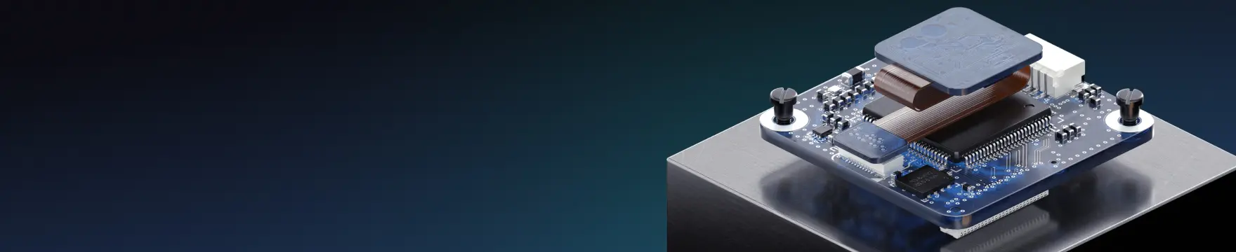
今すぐチーム間連携を強化し、設計プロセスを合理化しましょう。Altium Designerの高度な共同作業機能は、Altium 365とのシームレスな統合によりチーム間の連携作業を効率化します。Altium 365のクラウドプラットフォームを利用すると、必要なメンバーが、いつでもどこからでも設計データにアクセス可能。リアルタイムの共同作業により全員が常に同じ認識でプロジェクトを進められます。
今回のwebセミナーでは、以下のトピックを取り上げます:
Altium Designerによって変革されるチーム間連携が、PCB設計プロジェクトの効率をいかに改善されるかをご確認ください。

Registration has recently closed. Check back soon for on-demand webinar.


Altium DesignerとAltium 365を活用して、チームワークを効率化する方法をご紹介します。

Discover how to streamline teamwork using Altium Designer and Altium 365.

Discover how to streamline teamwork using Altium Designer and Altium 365.

Découvrez comment rationaliser votre travail d'équipe en utilisant Altium Designer et Altium 365.

Entdecken Sie, wie Sie die Teamarbeit mit Altium Designer und Altium 365 rationalisieren können.

Descubre cómo optimizar el trabajo en equipo con Altium Designer y Altium 365.

Altium Designer와 Altium 365를 사용하여 팀워크를 간소화하는 방법을 알아보세요.
ペースの速い産業用PCB設計の世界では、非効率なチーム連携が伝達ミス、バージョンコントロール、スケジュールや納期遅延など様々な問題を引き起こします。一元化されたシステムが整備されていないと、チーム間の重複作業や設計変更の矛盾、非効率的なコミュニケーションなどから多大な時間とコストを無駄にすることになります。
今すぐチーム間連携を強化し、設計プロセスを合理化しましょう。Altium Designerの高度な共同作業機能は、Altium 365とのシームレスな統合によりチーム間の連携作業を効率化します。Altium 365のクラウドプラットフォームを利用すると、必要なメンバーが、いつでもどこからでも設計データにアクセス可能。リアルタイムの共同作業により全員が常に同じ認識でプロジェクトを進められます。
今回のwebセミナーでは、以下のトピックを取り上げます:
Altium Designerによって変革されるチーム間連携が、PCB設計プロジェクトの効率をいかに改善されるかをご確認ください。

Daniel joined Altium in 2019 as an Application engineer and moved into the Technical Sales role in the same year. Daniel provides technical assistance for sales, third party distributors, and customers in the Asia Pacific region (APAC) and is based in the Altium Tokyo, Japan office. Daniel has experience with PCB, FPGA, and ASIC design in telecommunication and Information industries.

Alex has a background in electrical engineering and a strong passion for technical marketing. Graduating with a bachelor’s in electrical engineering from Clemson University in 2018, he has since excelled in various roles within the technology sector. Starting his career at Kyocera AVX, Alex served as an RF Field Applications Engineer, establishing strong client relationships and designing passive bandpass filters and antenna systems. He then transitioned to TDK as an Account Executive, where he provided sales and technical support, leading a dynamic sales team and offering design assistance to customers. Currently, Alex is a Technical Marketing Engineer at Altium, leveraging his technical expertise to develop marketing materials.

Jan Grooten is an Electronics Design Engineer who graduated (MScEE) in Asic design at the University of Twente, Netherlands. Besides Altium, Jan’s work experience includes Ericcsson, Sony and Plantronics where he served as Electronic System Engineer with focus on product development for Bluetooth headsets, with specialisation in small Li-ion batteries and Power management IC's. Jan started his career at Altium in 2017 as Field Application Engineer and is a Certified Interconnect Designer by IPC Council.

Nourhene is an Electronic Engineer specializing in PCB Design and FPGA Programming, holding a Master’s degree in RFID technologies. Since joining Altium in 2019, she has partnered closely with the sales team to support both prospects and existing customers through technical sales and marketing initiatives across Altium’s portfolio.
Before Altium, Nourhene designed complex PCBs for Automotive and Aerospace applications at large international companies, where she also managed comprehensive testing processes. She has extensive experience collaborating with PCB manufacturers across Europe and Asia. Nourhene holds CID certification and is a certified Altium Designer Trainer.

Martin Malenica has a masters in electronic and computer engineering at the University of Zagreb. His previous experience consists of multiple embedded systems positions at robotics start-ups (Gideon with USD 35m in Seed and Series-A funding) and SMEs. His engineering strengths lie in system architecture, PCB design and embedded programming. Aside from engineering, Martin has spent the last 1.5 years working at a leading European management consulting firm, where he focused on strategies to support large OEMs and Tier-1s regarding the current semiconductor shortage across the whole EMEA region. Martin has practical experience within AD, but also a good understanding of competitor tools, especially on the procurement and supply chain side, like Everstream, Resilinc, Silicon Expert, Z2Data etc. Martin Joined Altium in 2023 as part of the Technical Sales team in Germany.

Victor is a Field Applications Engineer (FAE) at Altium, where he combines technical expertise with a customer-centric approach. With over 10 years of developing electronics for the automotive and railway industry and two years of experience as a dedicated 3D-Electronics application engineer, establishing strong client relations within the EMEA and North American market. His primary focus is to ensure customer satisfaction by providing simple solutions to the customer's complex problems.

Aiden은 대학에서 전자공학을 전공하였으며 PCB 설계 분야의 R&D로 7년 이상의 경험을 가지고 있습니다. 그는 전자 제품을 위한 SMPS, 인버터, 컨버터 설계 경험이 있습니다. 제품 프로젝트를 이끌었으며 설계, 관리, 인증 제품 테스트와 같은 모든 작업을 경험했습니다. 그리고 한국 리셀러(Hancom Intelligence) 팀에서 4년 이상 Altium Designer 사용자들을 위한 기술 지원 및 교육을 제공했습니다. Concord Pro와 Altium 365를 사용하여 PLM 요구 사항에 대한 컨설팅 및 지원을 했습니다. 또한 Altium Designer에 대한 수십 차례의 교육 및 웨비나를 경험했습니다.
Aiden은 2022년 11월부터 Altium에서 기술 영업 엔지니어로 근무하고 있으며 현재 한국 사무소에 근무하고 있습니다.
はじめに
Simplify task management and enhance project visibility

Track everyone’s feedback in real-time and prevent errors that harm product quality.