


Altium Designer 24を最大限に活用する
Altium Designer 24で完全なシステム設計を実現
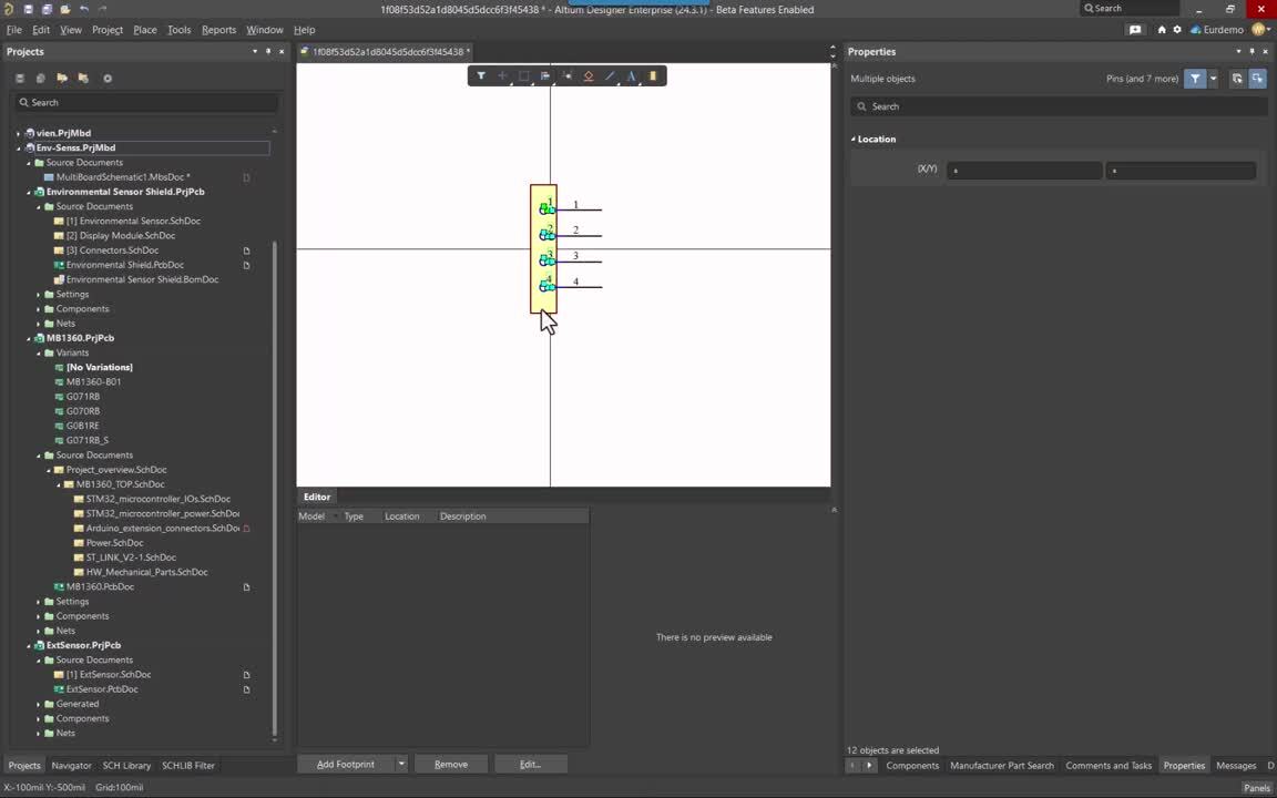
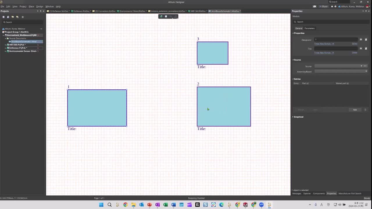
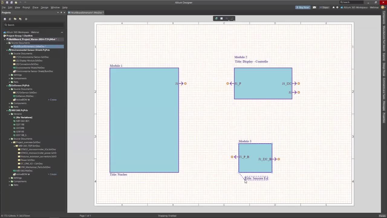
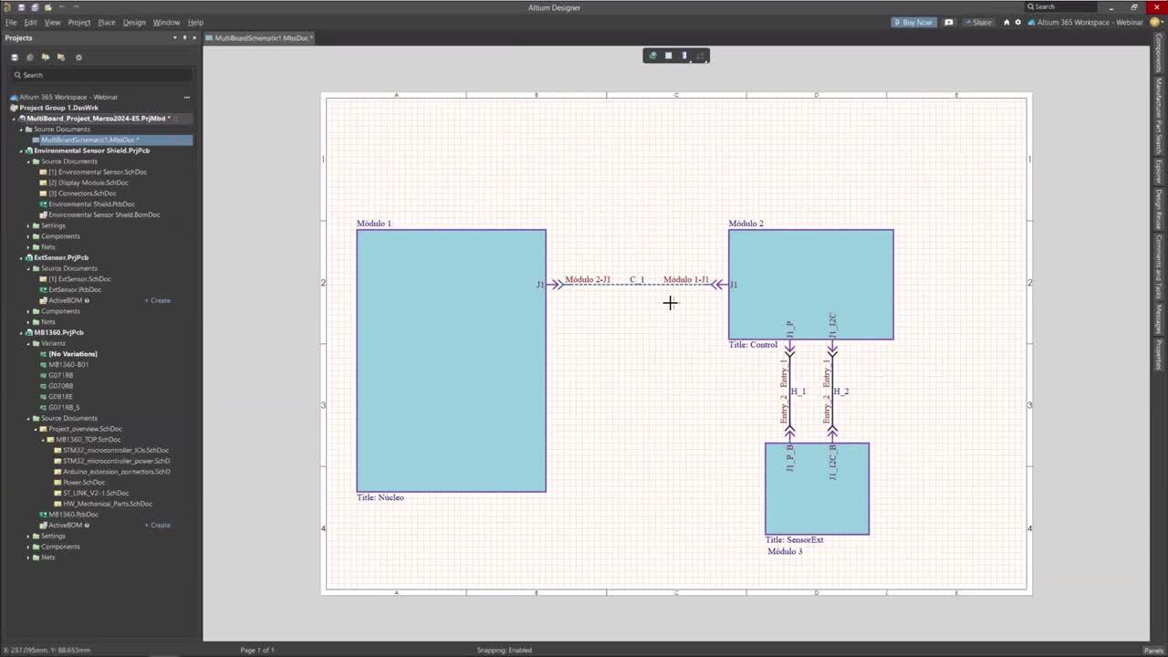
急速に進化する技術環境では、極めて効率的で適応性のある電子システムを設計する能力が最優先されます。ハーネス、マルチボード、MCAD CoDesignerなどの機能を利用できない場合、プロジェクトで大きな問題に直面する恐れがあります。こうしたツールがなければ、納期の遅れ、設計エラーの増加、電気的側面と機構的側面の同期の欠如につながり、プロジェクト全体の成功を妨げることになります。
設計の複雑性を解消する準備はできていますか? Altium Designer 24では、設計の方法を改革することができます。今すぐご登録のうえ、ハーネスデザイン、マルチボードなどの機能や、MCAD CoDesignerを使用した機構設計者との共同作業のためにAltium Designer 24が提供する包括的なソリューションをご確認ください。
次回のWEBセミナーでは次の内容について解説します。
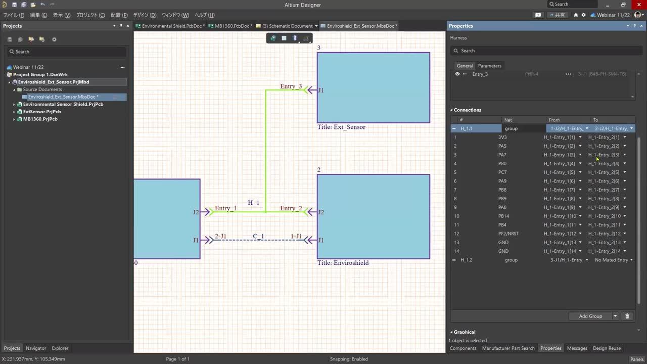
- Altium Designer 24でのハーネスデザイン
- 統合環境でのマルチボードデザイン
- MCAD CoDesignerとのシームレスな統合

Registration has recently closed. Check back soon for on-demand webinar.
Related Technical Documentation
関連リソース
Altium Designer 24で完全なシステム設計を実現
投稿日 March 21, 2024

At a Glance
今回のWebセミナーに参加すると、設計ワークフローの最適化、生産性の向上、マルチボードデザイン プロジェクトで発生する一般的な問題の解消に関する貴重な洞察を入手できます。


-
 プレゼンター:ダニエル チョウ
 01:07:41
•
Mar 20, 2024
プレゼンター:ダニエル チョウ
01:07:41
•
Mar 20, 2024
01:07:41
•
Mar 20, 2024
プレゼンター:ダニエル チョウ
01:07:41
•
Mar 20, 2024
-
 Hosted by Alex Hall - Technical Marketing Engineer
00:33:46
•
Mar 22, 2024
Hosted by Alex Hall - Technical Marketing Engineer
00:33:46
•
Mar 22, 2024
Hosted by Alex Hall - Technical Marketing Engineer
00:33:46
•
Mar 22, 2024
Hosted by Alex Hall - Technical Marketing Engineer
00:33:46
•
Mar 22, 2024
-
 Hosted by Aida Gharahkhani - Field Application Engineer
00:48:52
•
Mar 21, 2024
Hosted by Aida Gharahkhani - Field Application Engineer
00:48:52
•
Mar 21, 2024
Hosted by Aida Gharahkhani - Field Application Engineer
00:48:52
•
Mar 21, 2024
Hosted by Aida Gharahkhani - Field Application Engineer
00:48:52
•
Mar 21, 2024
-
 Présenté par Nourhene Kerkeni - Field Application Engineer
00:33:36
•
Mar 29, 2024
Présenté par Nourhene Kerkeni - Field Application Engineer
00:33:36
•
Mar 29, 2024
Présenté par Nourhene Kerkeni - Field Application Engineer
00:33:36
•
Mar 29, 2024
Présenté par Nourhene Kerkeni - Field Application Engineer
00:33:36
•
Mar 29, 2024
-
 Präsentiert von Martin Malenica - Field Application Engineer
00:22:58
•
Mar 28, 2024
Präsentiert von Martin Malenica - Field Application Engineer
00:22:58
•
Mar 28, 2024
Präsentiert von Martin Malenica - Field Application Engineer
00:22:58
•
Mar 28, 2024
Präsentiert von Martin Malenica - Field Application Engineer
00:22:58
•
Mar 28, 2024
-
 오힘찬 FAE 발표
00:40:11
•
Mar 25, 2024
오힘찬 FAE 발표
00:40:11
•
Mar 25, 2024
오힘찬 FAE 발표
00:40:11
•
Mar 25, 2024
오힘찬 FAE 발표
00:40:11
•
Mar 25, 2024
-
 Presentato da Manuel Valero - Field Application Engineer
00:47:54
•
Mar 25, 2024
Presentato da Manuel Valero - Field Application Engineer
00:47:54
•
Mar 25, 2024
Presentato da Manuel Valero - Field Application Engineer
00:47:54
•
Mar 25, 2024
Presentato da Manuel Valero - Field Application Engineer
00:47:54
•
Mar 25, 2024
-
 Presentado por Manuel Valero - Field Application Engineer
00:47:27
•
Mar 22, 2024
Presentado por Manuel Valero - Field Application Engineer
00:47:27
•
Mar 22, 2024
Presentado por Manuel Valero - Field Application Engineer
00:47:27
•
Mar 22, 2024
Presentado por Manuel Valero - Field Application Engineer
00:47:27
•
Mar 22, 2024
Product:
マルチボード
Harness Design
Altium Designer
ウェビナー
電気技術者
Systems and Product Design
Other Recordings
急速に進化する技術環境では、極めて効率的で適応性のある電子システムを設計する能力が最優先されます。ハーネス、マルチボード、MCAD CoDesignerなどの機能を利用できない場合、プロジェクトで大きな問題に直面する恐れがあります。こうしたツールがなければ、納期の遅れ、設計エラーの増加、電気的側面と機構的側面の同期の欠如につながり、プロジェクト全体の成功を妨げることになります。
設計の複雑性を解消する準備はできていますか?

Author
Author
Daniel joined Altium in 2019 as an Application engineer and moved into the Technical Sales role in the same year. Daniel provides technical assistance for sales, third party distributors, and customers in the Asia Pacific region (APAC) and is based in the Altium Tokyo, Japan office. Daniel has experience with PCB, FPGA, and ASIC design in telecommunication and Information industries.

Author
Author
Alex has a background in electrical engineering and a strong passion for technical marketing. Graduating with a bachelor’s in electrical engineering from Clemson University in 2018, he has since excelled in various roles within the technology sector. Starting his career at Kyocera AVX, Alex served as an RF Field Applications Engineer, establishing strong client relationships and designing passive bandpass filters and antenna systems. He then transitioned to TDK as an Account Executive, where he provided sales and technical support, leading a dynamic sales team and offering design assistance to customers. Currently, Alex is a Technical Marketing Engineer at Altium, leveraging his technical expertise to develop marketing materials.

Author
Author
Aida works as a Technical Sales Engineer at Altium and is based in the Sydney, Australia office. Aida studied Electrical/Electronic Engineering and completed Master of Engineering (MEng) Field of Mechatronics, Robotics, and Automation Engineering from the University of Western Sydney (UWS). Aida also completed certificates in Microcontroller Programming, Project Management Principles and Practices Specialization from the university of UC Irvine California. Aida has experience as an Electrical Engineer, Business Development Manager, Project Manager, Operations Manager, most recently in the last 10 years prior to joining Altium working in Engineering Process improvement. The most important thing that she always focuses on in her career is communication and trust. Aida strongly believes that communication is the solvent of all problems, when the trust accountability is high, communication is easy, instant, and effective.

Author
Author
Nourhene is an Electronic Engineer specializing in PCB Design and FPGA Programming, holding a Master’s degree in RFID technologies. Since joining Altium in 2019, she has partnered closely with the sales team to support both prospects and existing customers through technical sales and marketing initiatives across Altium’s portfolio.
Before Altium, Nourhene designed complex PCBs for Automotive and Aerospace applications at large international companies, where she also managed comprehensive testing processes. She has extensive experience collaborating with PCB manufacturers across Europe and Asia. Nourhene holds CID certification and is a certified Altium Designer Trainer.

Author
Author
Martin Malenica has a masters in electronic and computer engineering at the University of Zagreb. His previous experience consists of multiple embedded systems positions at robotics start-ups (Gideon with USD 35m in Seed and Series-A funding) and SMEs. His engineering strengths lie in system architecture, PCB design and embedded programming. Aside from engineering, Martin has spent the last 1.5 years working at a leading European management consulting firm, where he focused on strategies to support large OEMs and Tier-1s regarding the current semiconductor shortage across the whole EMEA region. Martin has practical experience within AD, but also a good understanding of competitor tools, especially on the procurement and supply chain side, like Everstream, Resilinc, Silicon Expert, Z2Data etc. Martin Joined Altium in 2023 as part of the Technical Sales team in Germany.

Author
Author
Aiden은 대학에서 전자공학을 전공하였으며 PCB 설계 분야의 R&D로 7년 이상의 경험을 가지고 있습니다. 그는 전자 제품을 위한 SMPS, 인버터, 컨버터 설계 경험이 있습니다. 제품 프로젝트를 이끌었으며 설계, 관리, 인증 제품 테스트와 같은 모든 작업을 경험했습니다. 그리고 한국 리셀러(Hancom Intelligence) 팀에서 4년 이상 Altium Designer 사용자들을 위한 기술 지원 및 교육을 제공했습니다. Concord Pro와 Altium 365를 사용하여 PLM 요구 사항에 대한 컨설팅 및 지원을 했습니다. 또한 Altium Designer에 대한 수십 차례의 교육 및 웨비나를 경험했습니다.
Aiden은 2022년 11월부터 Altium에서 기술 영업 엔지니어로 근무하고 있으며 현재 한국 사무소에 근무하고 있습니다.

Author
Author
Manuel Valero is an Electronics Engineer with experience ranging from his own repair and IT businesses to working with multinational companies in the semiconductor and passive components branches; he has covered diverse roles like Repair Engineer, Product Engineer, Testing Engineer, Design Engineer, Product Marketing Engineer, FDE, etc.
He has quite varied interests, not just the electronics area; this go from bicycle riding, swimming, wandering, astrophysics, physics, biology and a long etcetera.
Having worked and lived in several countries, he finds himself comfortable in multicultural environments and enjoys working with customers.
Related Technical Documentation
関連リソース
設計からリリースまで、摩擦なく。
- レビューを適切なバージョンに紐づけ
- 引き継ぎ時の混乱や手戻りを削減
- 調達やリリースのリスクを早期に発見
- 必要に応じて共有しながら、1人でも作業可能
はじめに
Platform-based Solutions
Tools
ソリューション
会社情報
採用情報